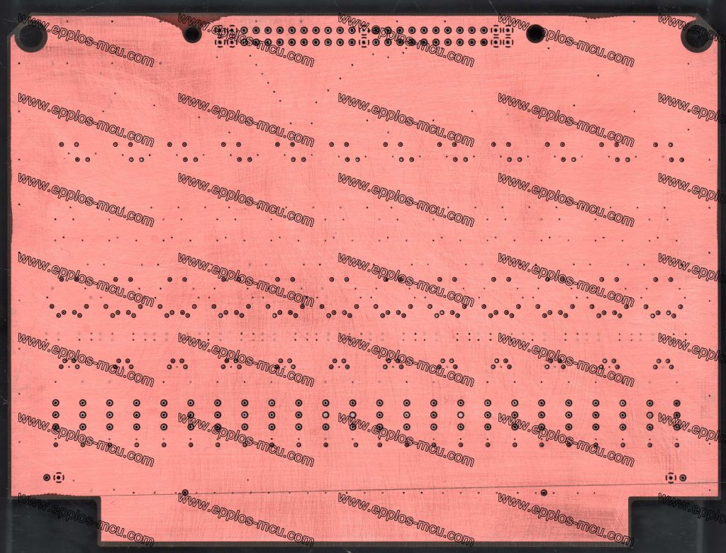
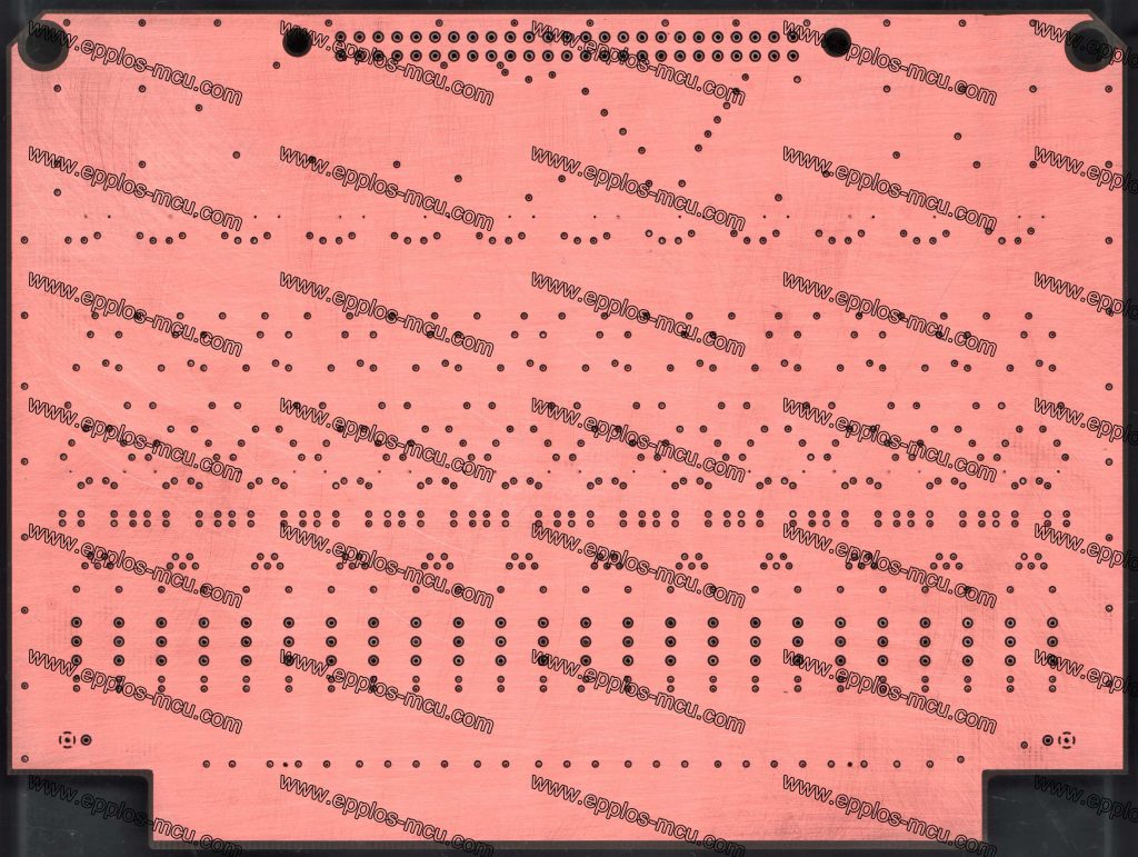
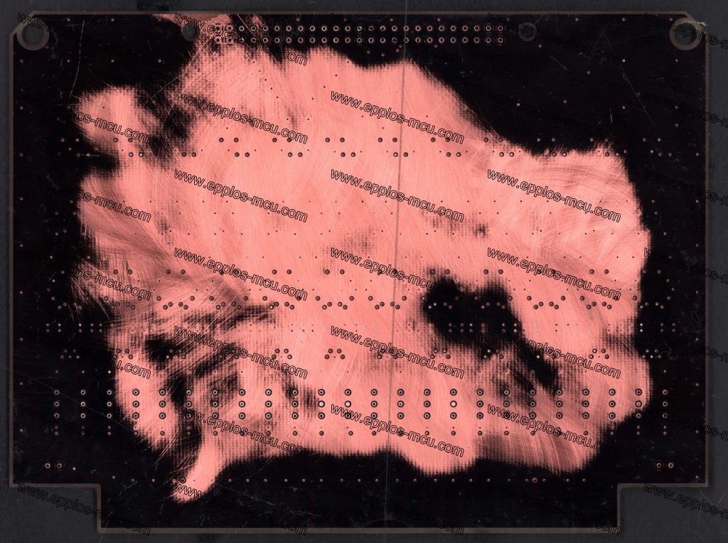
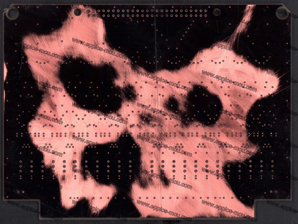
Blog Your current location is : Home Blog EPPLOS Blog A 4-Layer PCB reverse engineering successfully A 4-Layer PCB reverse engineering successfully By admin 9月 17, 2021 2207 FacebookemailTwitterLinkedin This is a four layers pcb reverse engineering for pcb file,BOM and schematic successfully with 7-10 days. For more information and details,please feel free to get contact with me jerry@epplos-mcu.com . Previous: How to work with us ? Next: IC Decap and IC Die photos
A 4-Layer PCB reverse engineering successfully By admin 9月 17, 2021 2207 FacebookemailTwitterLinkedin This is a four layers pcb reverse engineering for pcb file,BOM and schematic successfully with 7-10 days. For more information and details,please feel free to get contact with me jerry@epplos-mcu.com .